Semiconductor & Advanced Materials Analysis
Precision Materials Characterization | Failure Analysis | Cross-Sectioning | R&D Services
State of the Art Semiconductor Analysis Services
Phineas Laboratory provides comprehensive semiconductor analysis services and develops advanced sensor technologies for defense and first responder applications.
Our facility combines state-of-the-art analytical equipment with deep technical expertise to support failure analysis, materials characterization, and product development across multiple industries.
Scanning Electron Microscopy
2-3nm resolution imaging with EDS analysis
Precision Cross-Sectioning
Broad ion milling cross-section of Au bond wires, semiconductor packaging, and more..
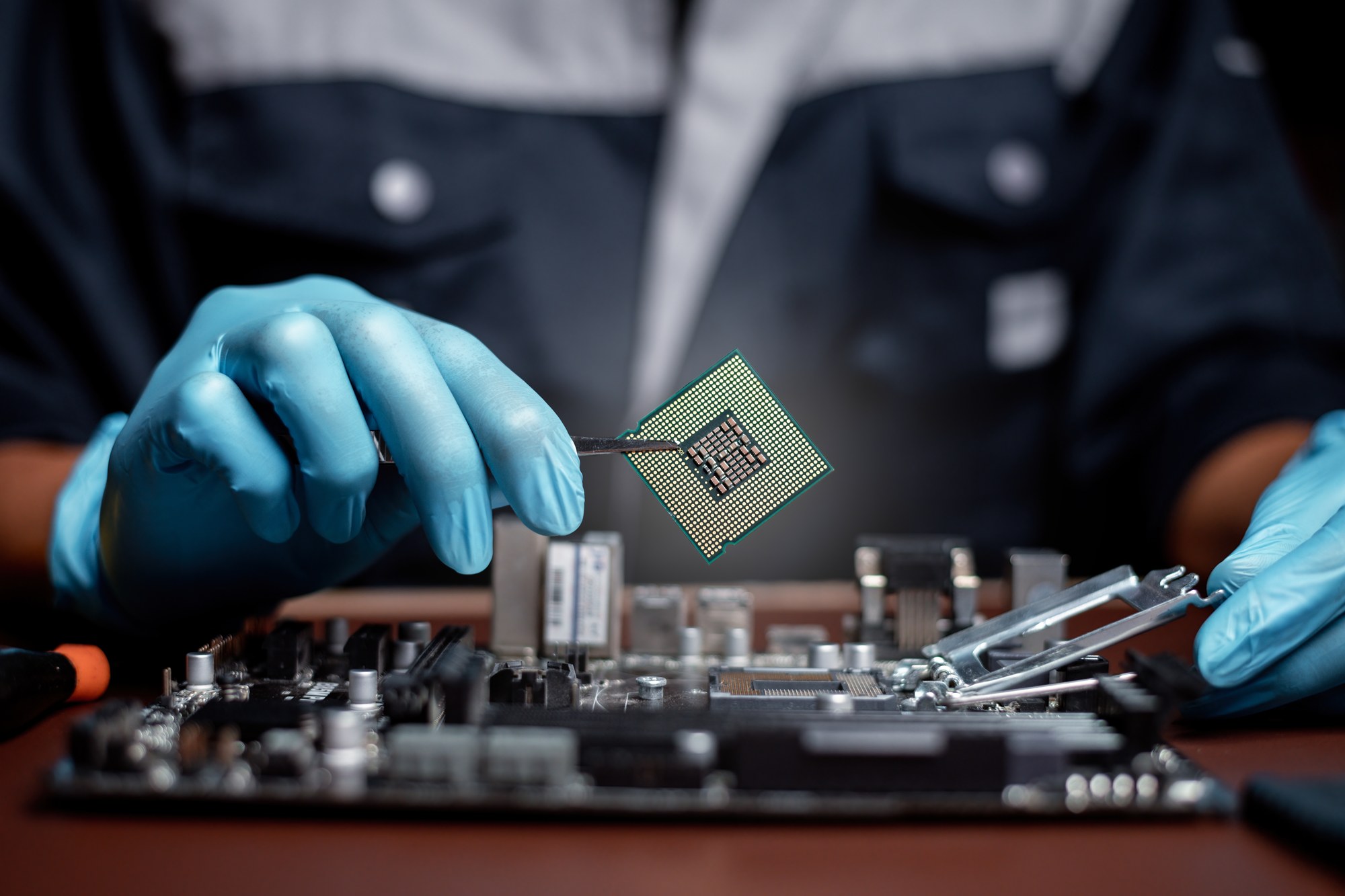
Failure Analysis
Root cause determination and reliability testing
??????????????????????????????????????????????????????????????????????????????????????????????????????????????????????????????????????????????????????????????????????????????????????????????????????????????????????????????????????????????????????????????????????????????????????????????????????????? TEM Wedge Sample Preparation
Two sided thinning with 1° wedge angle to produce electron transparent specimens from bulk metals, thin films, and semiconductors. Submicron tip thickness with enough base material for safe handling and TEM loading.
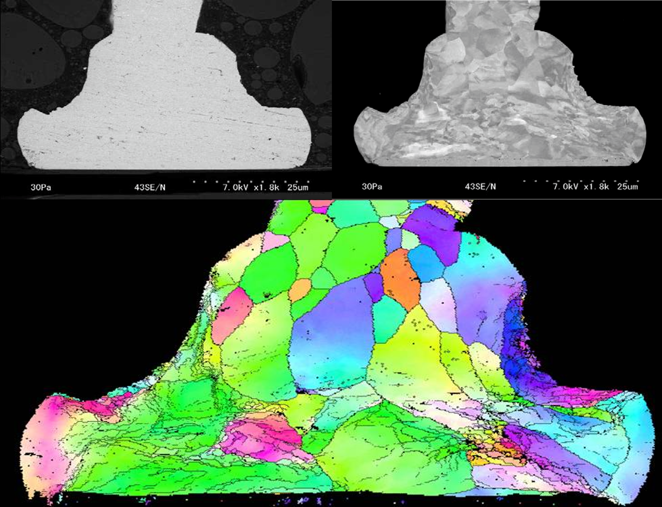
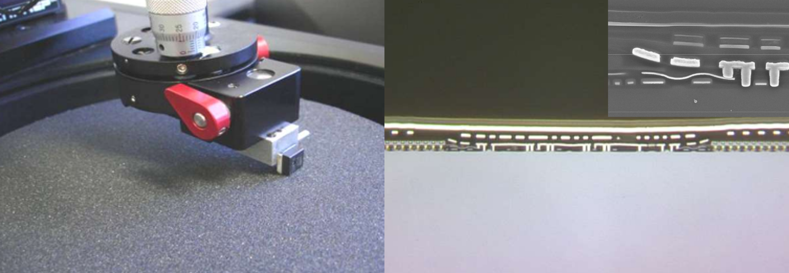
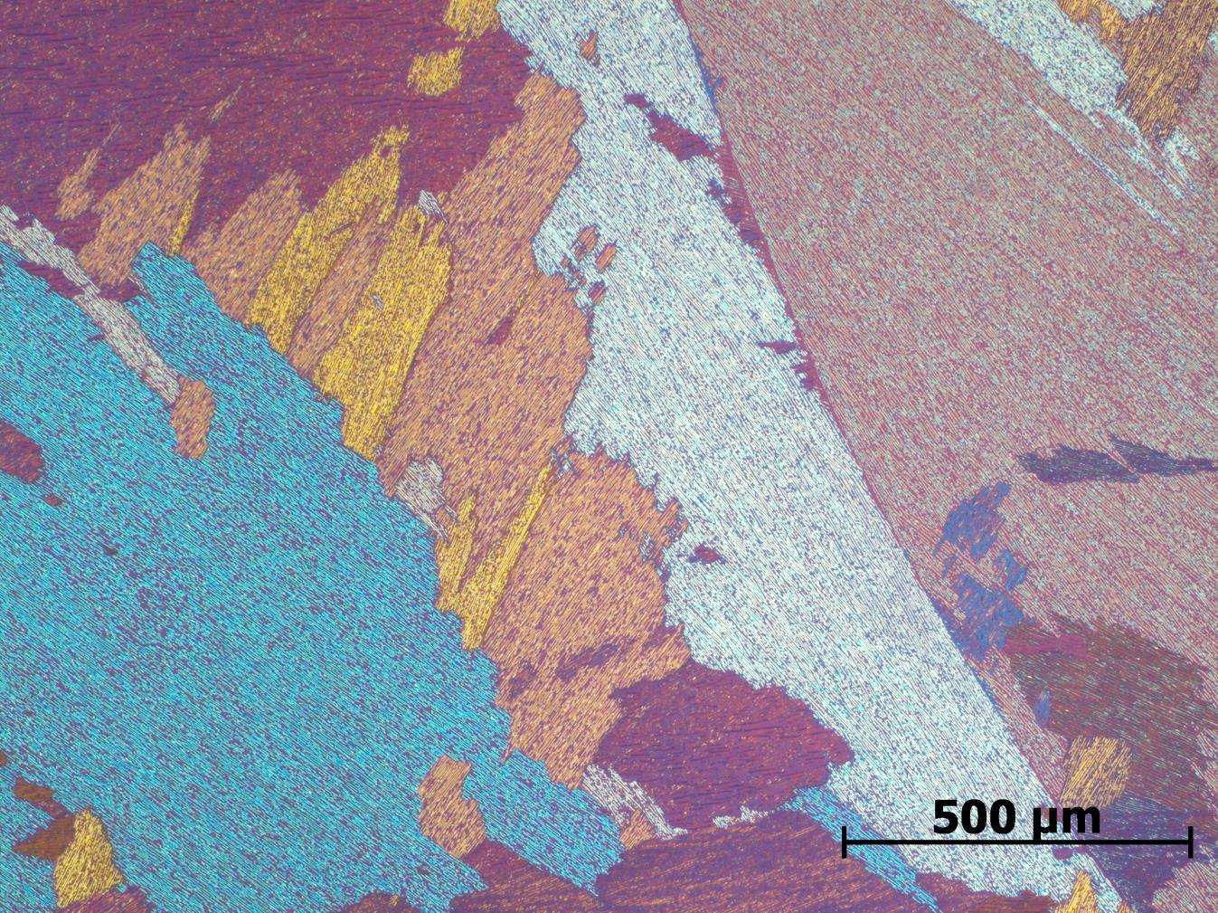
Broad Ion Beam Cross-Sectioning
ArBlade 5000 BIB milling produces large area, contamination-free cross sections without the mechanical or chemical damage of traditional polishing.
Faster than FIB for site specific lamella preparation, with no smearing, curtaining, or deformation at the cut face.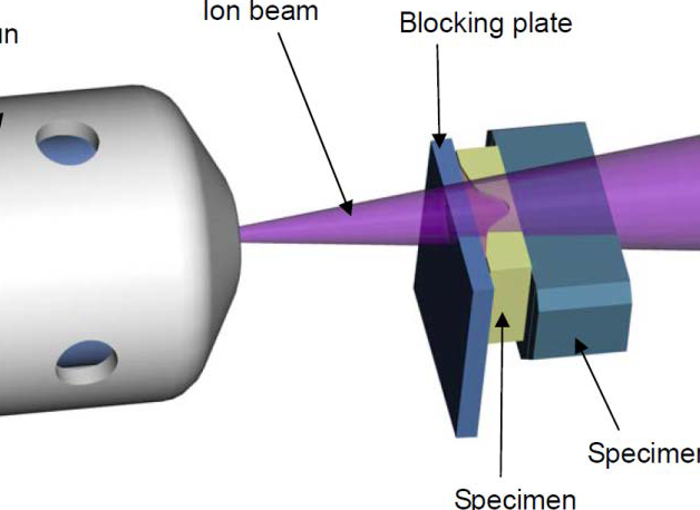
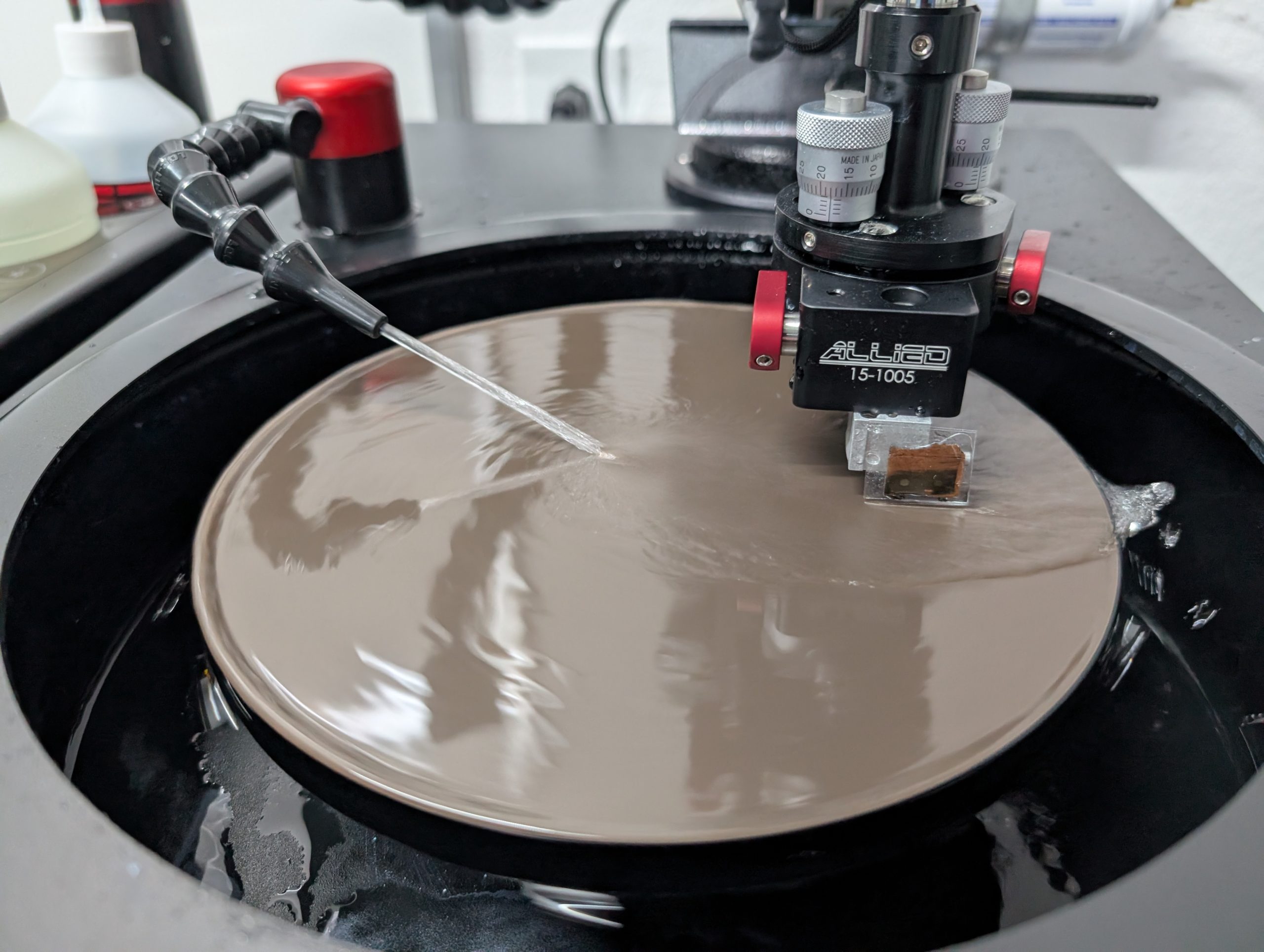
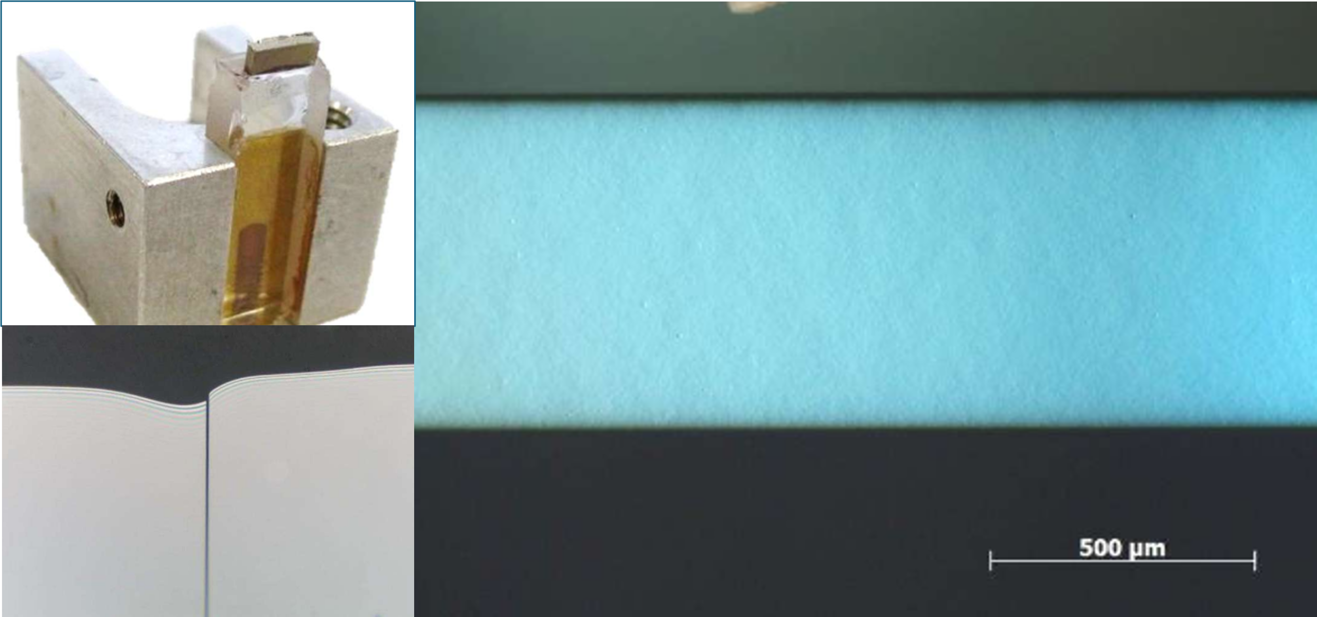
SIMS Backside Sample Preparation
Backside thinning of silicon to 0.5 µm for SIMS depth profiling, verified in real time using transmitted light interference fringes. Eliminates front side ion yield transient artifacts.
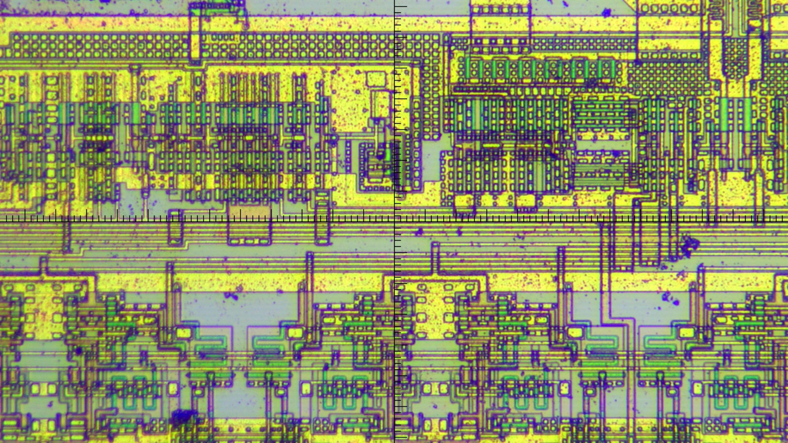
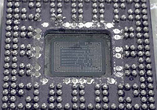
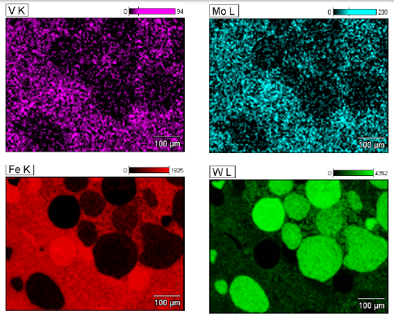
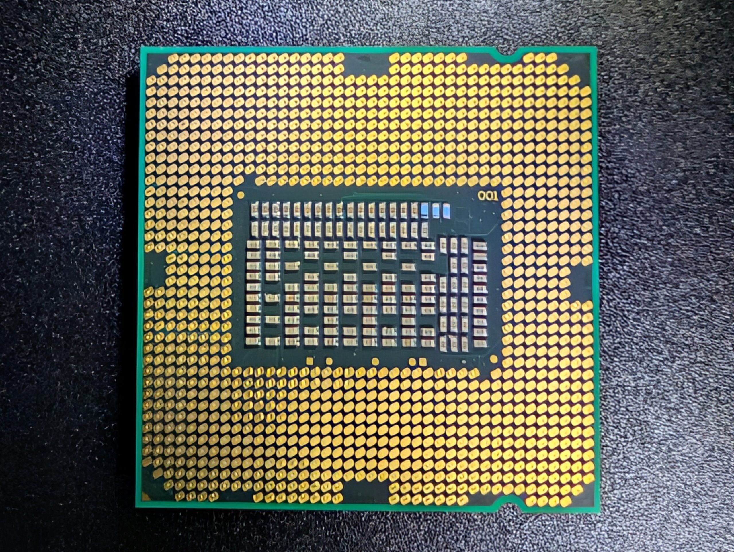
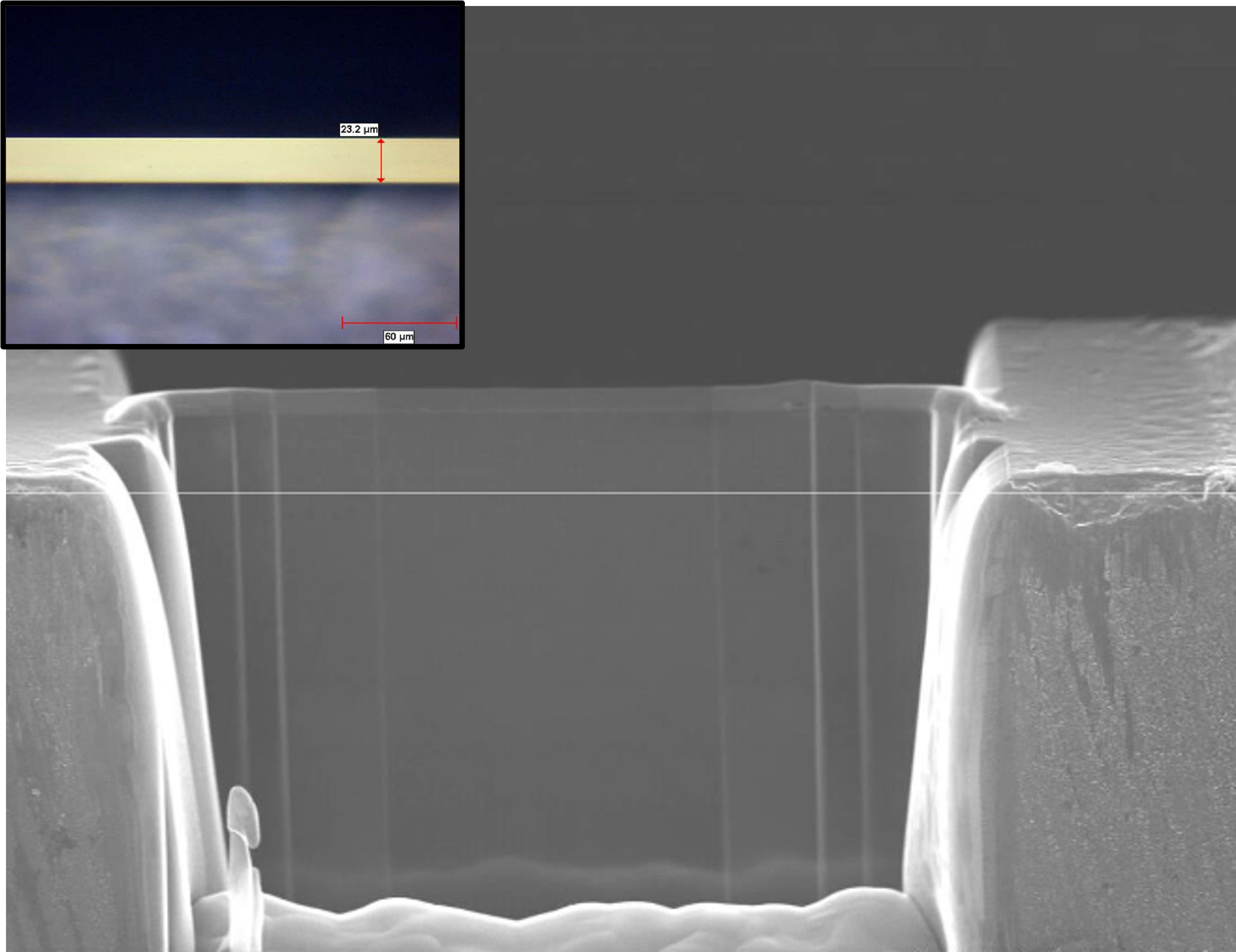
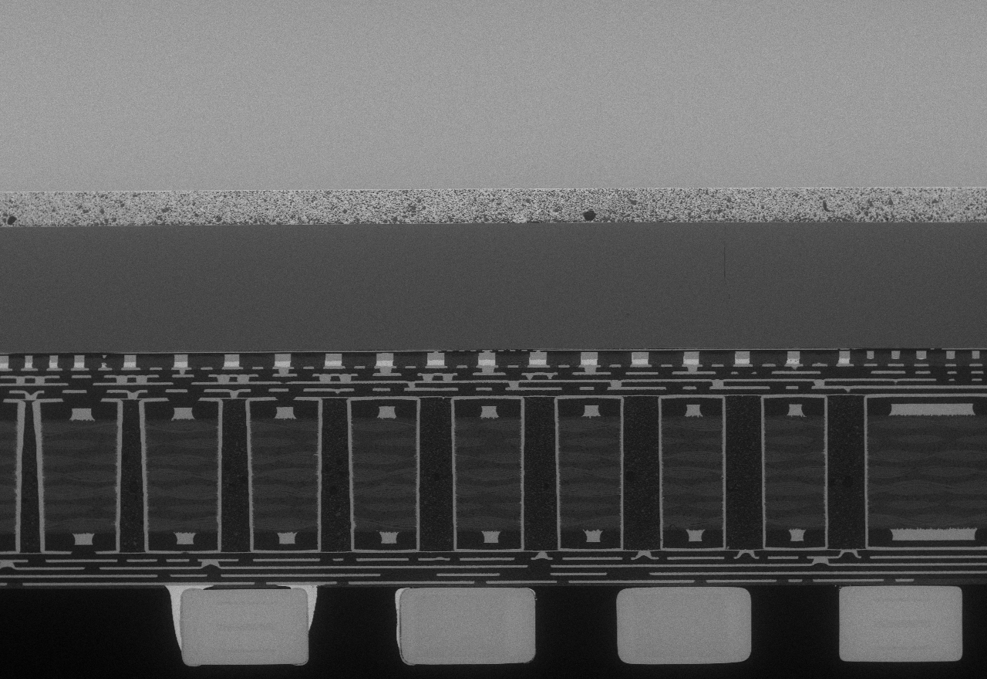
Microelectronic Device Cross-Sectioning
Precision cross-sectioning of dies, BGAs, packages, bond wires, and solder bumps to the feature level. Polishing tailored to multi-material systems including gold, copper, solder, and nickel.
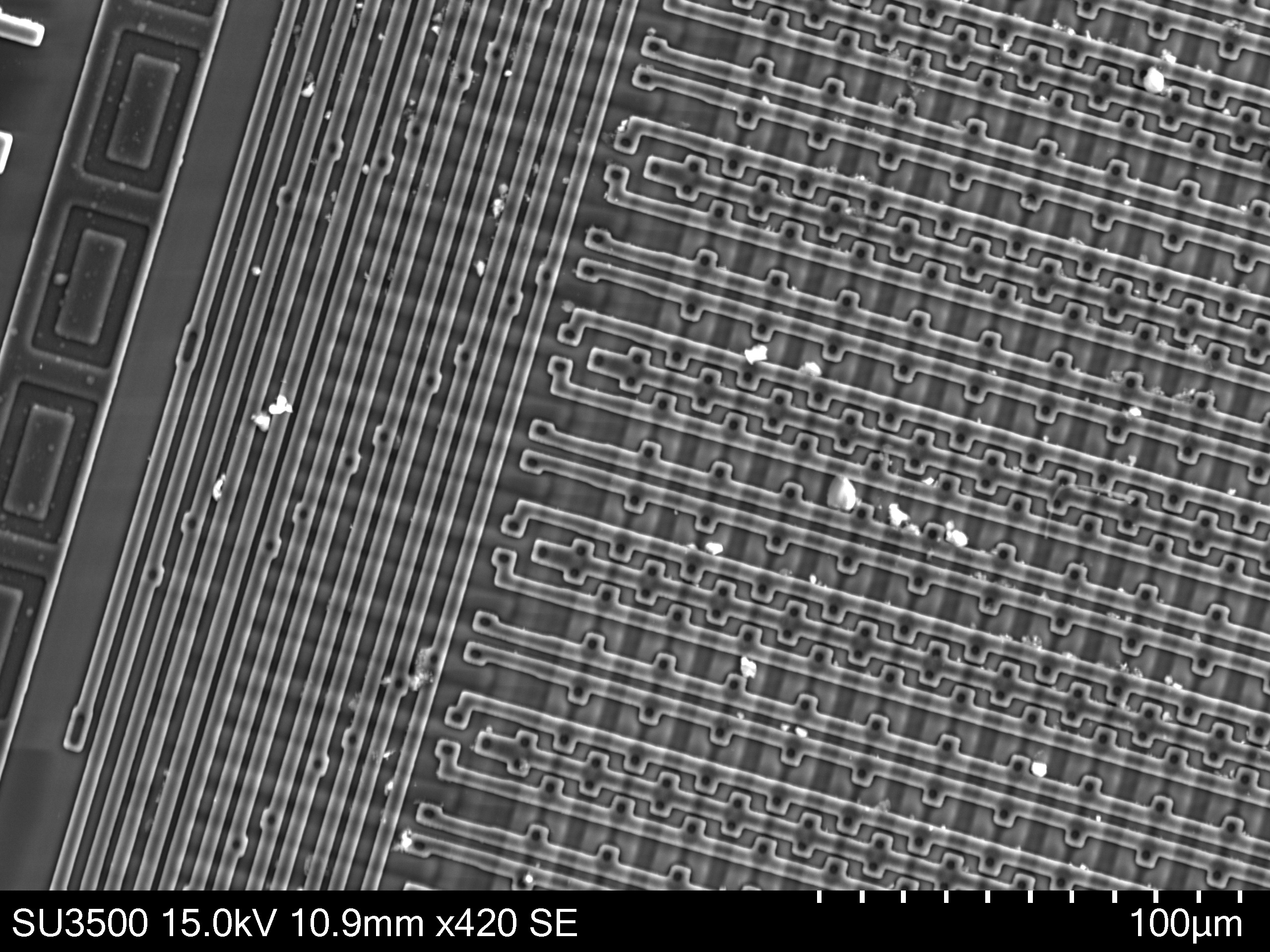
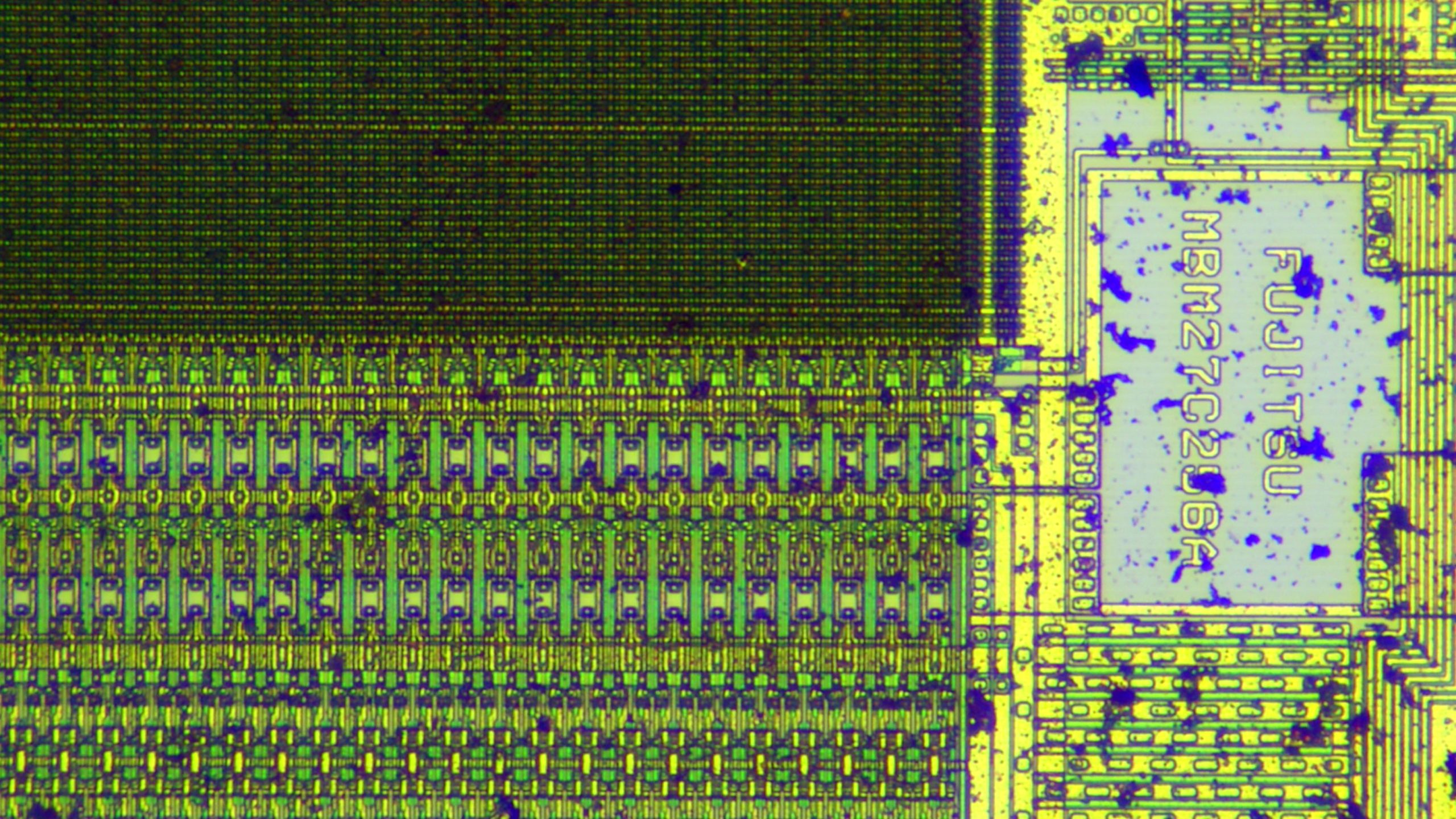
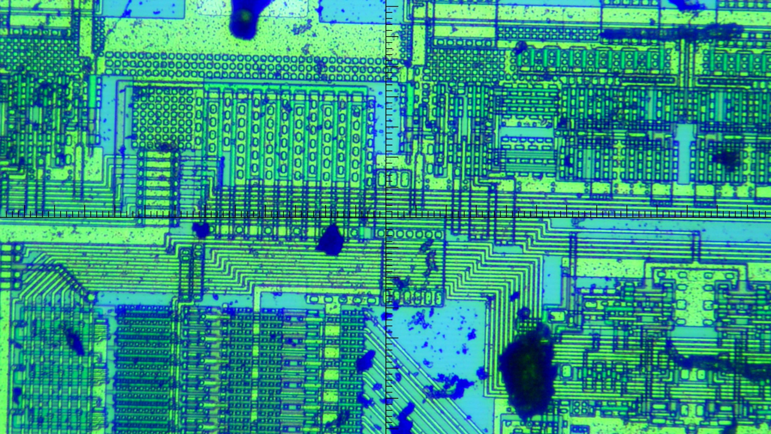
IC Parallel Delayering
Layer by layer removal of IC metallization and dielectrics through precision parallel polishing. Exposes each interconnect level for circuit extraction, design verification, or hardware assurance inspection.
Custom R&D Projects
Sensor development and materials research
Pre-fib thinning
Mechanical thinning to minimize FIB mill time and improve lamella quality

Our Semiconductor Services for Multiple Applications
- Semiconductor Manufacturing
- Defense & Aerospace
- Automotive Electronics
- Medical Devices
- Research Institutions