From surface morphology to subsurface defects, our electron microscopy imaging process will identify surface characteristics of your sample.
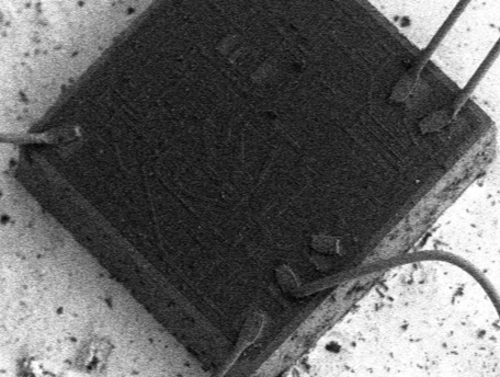
Wire bond integrity, die attach quality, package delamination, and semiconductor junction analysis.
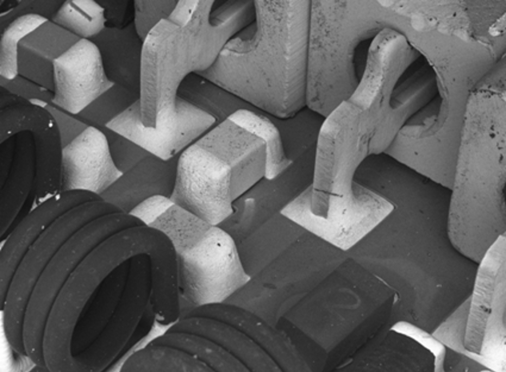
Crystal structures, grain boundaries, phase distributions, and microstructural features that determine material properties.
Critical dimensions, coating thickness, particle size distribution, and feature measurements at nanoscale.
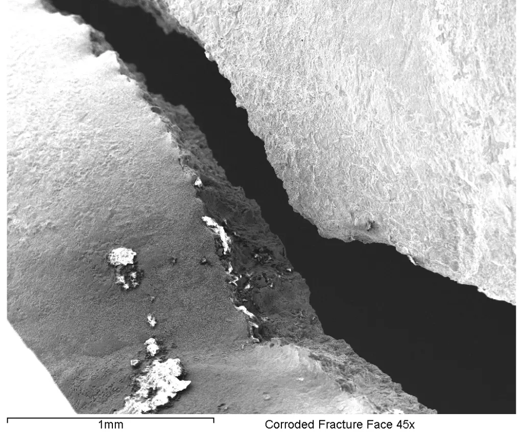
Crack initiation points, fracture surfaces, corrosion patterns, and wear mechanisms that explain why components fail.
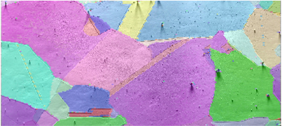
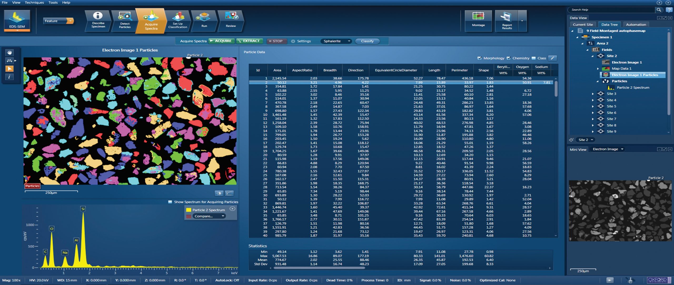
EDS mapping for elemental distribution, compositional analysis, and identification of unknown materials.
Simple, transparent, and fast.
Share your imaging needs and sample details.
Receive pricing within 24 hours.
Send via your preferred carrier.
Our technicians will capture your images and characterize the results for you.
High-res images + analysis report.