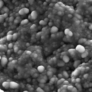
Description
Multiple images are taken to get a good picture of the sample. An EDS mapping, line scan, or point measurement is collected to measure the sample composition (elemental at.% or wt.% per um).
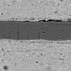
The sample can be prepared with a metallic coating for non-conductive samples.
For cross-section measurement, additional preparation might be needed using: Ion-Beam Milling
Difference between SEM-EDS Imaging and SEM Imaging is that SEM-EDS Imaging comes with sample composition and elemental composition maps of the sample.